
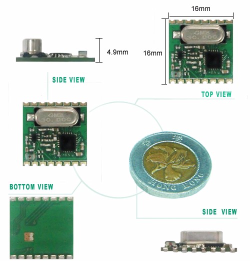
APPEARANCE
產品外觀


FEATURES
產品特色


SPECIFICATION
產品規格
Worldwide 433 ISM band operation
0.123 to 256Kbps on air datarates
Ultra low power operation
Output power range +20 dBm Max
18.5 Ma receive, 85mA @ +20dBm transmit
Low cost
Digital RSSI
FSK, GFSK, and OOK modulation
1.8 to 3.6V supply range
Temperature sensor and 8-bit ADC
Automatic packet handling
Auto packet transaction handling
TX and RX 64 byte FIFOs
On-chip crystal tuning
| Parameter | Symbol | Test Condition | Min | Typ | Max | Unit |
|---|---|---|---|---|---|---|
| Supply Voltage Range | Power | 1.8 | 3 | 3.6V | V | |
| Power Down | Power | Power Down | 15 | nA | ||
| RX Mode Current | Receiver | 1Kbps | 18.5 | mA | ||
| TX Mode Current | Transmitter | 20dBm | 85 | mA | ||
| RX Sensitivity | Receiver | 512bps 433MHz | -121dBm | dBm |
| Pin | Name | I/O | Description |
|---|---|---|---|
| 1 | Antenna | Input/output | Antenna |
| 2 | GND | GND | Ground |
| 3 | ANT RX | Input | Controlled antenna switch, IF Receiver MODE IS High Voltage |
| 4 | ANT TX | Input | Controlled antenna switch, IF Transmitter MODE IS High Voltage |
| 5 | VCC | Input | +1.8V to +3.6 V Supply Voltage Input to Internal Regulators |
| 6 | GPIO0 | Digital I/O | General Purpose Digital I/O that may be configured through the registers to perform various functions |
| 7 | GPIO1 | Digital I/O | |
| 8 | GPIO2 | Digital I/O | |
| 9 | GND | GND | Ground |
| 10 | SDO | Digital Output | Provides a serial read back function of the internal control registers. |
| 11 | SDI | Digital Input | This pin provides the serial data stream for the 4-line |
| 12 | SCLK | Digital Input | Serial Clock Input. |
| 13 | nSEL | Digital Input | Serial Interface *** input. 0– VDD V digital input. This pin provides the ***/Enable function for the 4-line serial data bus. The signal is also used to signify burst read/write mode |
| 14 | NIRQ | Digital Output | General Microcontroller Interrupt Status output. When the Si4430/31/32 exhibits anyone of the Interrupt |
| 15 | SDN | Digital Input | Shutdown input pin. 0–VDD V digital input. SDN should be = 0 in all modes except Shutdown mode. When SDN =1 the chip will be completely shut down and the contents of the registers will be lost. |
| 16 | GND | GND | Ground |